New memory MRAM (1): technical analysis
Time:2018-10-30
MRAM
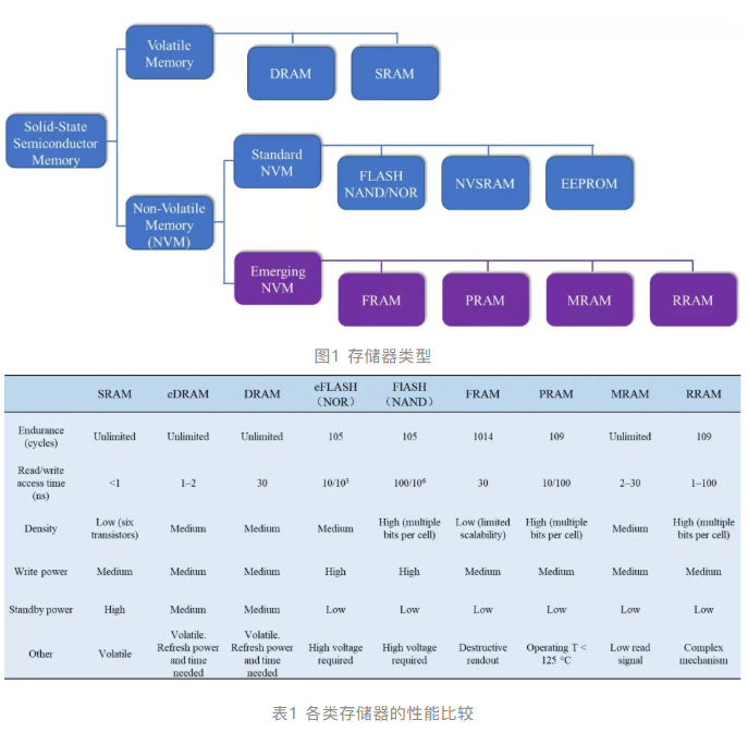
Magnetic random access memory (MRAM) is one of the new non-volatile random access memory (NVRAM) based on the principle of reading reluctance (RR) (Fig. 1). Compared with other storage technologies (Table 1), MRAM achieves a better compromise in speed, area, number of writes and power consumption. Therefore, it is considered as one of the potential access devices to construct the next generation non-volatile cache and main memory.
 Magnetic tunnel junction and tunneling magnetoresistance
The performance of MRAM is improved due to the continuous increase of the tunneling magnetoresistance (TMR) value of the Magnetic Tunnel Junction (MTJ). The magnetic tunnel junction is the basic memory cell of MRAM. The core part is composed of two ferromagnetic metal layers (typically 1~2.5nm) sandwiching a tunneling barrier layer (insulation material, typical thickness is 1~1.5nm) A nano-multilayer film similar to a sandwich structure is formed (Fig. 2). One of the ferromagnetic layers is called a reference layer or a pinned layer, and its magnetization is fixed along the direction of the easy magnetization axis.

Another ferromagnetic layer is called the Free Layer, and its magnetization has two stable orientations, which are parallel or anti-parallel to the reference layer, respectively, which will make the magnetic tunnel junction in a low-resistance state or a high-impedance state. The phenomenon is called tunneling magnetoresistance. The two resistance states can represent binary data "0" and "1", respectively, which is the basic principle of MRAM storage.
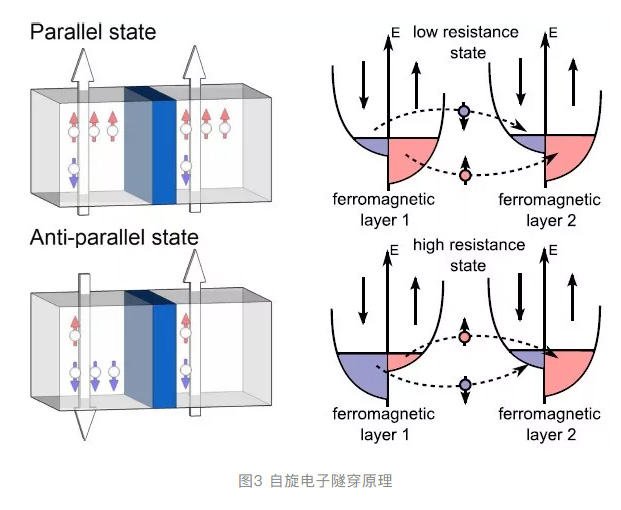
The tunneling magnetoresistance effect can be explained by the spin-dependent tunneling theory. As shown in Fig. 3, for ferromagnetic metals, the spin-up and spin-down electronic states are unevenly distributed around the Fermi level. When the reference layer is in the same direction as the magnetization direction of the free layer, the electron spin directions in the majority of the two ferromagnetic materials are the same, the tunneling probability is high, the tunneling current is large, and the magnetic tunnel junction exhibits a low resistance state; The tunnel junction exhibits a high resistance state.
The tunneling magnetoresistance effect was first observed in 1975 by the French scholar Julilere at low temperatures, but it did not attract much attention at that time. The research progress since then was extremely slow, because the process level at that time was difficult to produce high quality. Nano film.
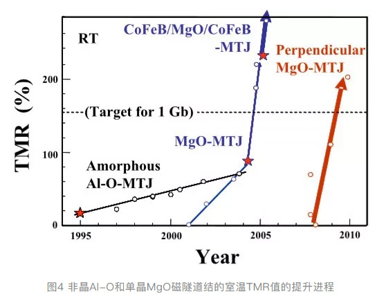
As shown in Figure 4, until 1995, Miyazaki of Tohoku University and MIT Moodera of the United States successfully obtained the tunneling magnetoresistance effect at room temperature. The magnetic tunnel junctions prepared by them used Al2O3 as a barrier and TMR values were respectively It is 11.8% and 18%. This achievement has revived the enthusiasm for research on tunneling magnetoresistance.
Subsequently, in order to further promote the application of magnetic tunnel junctions in the field of hard disk heads and MRAM (which requires a TMR value of about 150% or higher at room temperature), the academic community has conducted extensive exploration to obtain higher TMR values. In 2001, Butler and Mathon et al. theoretically predicted that if the barrier of the magnetic tunnel junction is replaced by amorphous Al2O3 to single crystal MgO, a higher TMR value will be obtained (theoretical prediction can reach 1000%). It is the symmetry of the MgO lattice that has a screening effect on the wave function of the tunneling electrons, which has an additional contribution to the TMR.
This theoretical prediction was confirmed in 2004: Parkin et al. of IBM Laboratories and Yuasa et al. of AIST Research Institute of Japan successfully prepared a magnetic tunnel junction using a single-crystal MgO barrier, and the room temperature TMR value reached about 200%. Since then, the experimental value of the room temperature TMR of the magnetic tunnel junction based on the single crystal MgO barrier has been increasing, reaching 604% at one time (2008). The current mainstream magnetic tunnel junctions use single crystal MgO as a barrier layer.
 Classification and development of MRAM
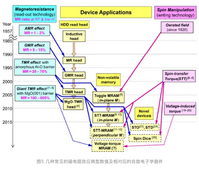
Based on TMR and Giant TRM (TMR>100%) effects, a total of two generations of major MRAM device types have been derived (Figure 5): The first generation is a magnetic field-driven MRAM, which is driven by a magnetic field generated by a current. The magnetic moment of the storage unit is written, typically representing a star MRAM (astroid-MRAM) and a nested MRAM (toggle-MRAM); the second generation is a current-driven spin transfer torque MRAM (Spin Transfer Torque MRAM, STT-MRAM), which writes the memory cell by polarization current.
1. astroid-MRAM and toggle-MRAM
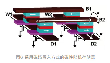
The write operation of the MRAM is achieved by magnetization flipping of the free layer in the magnetic tunnel junction. One of the simplest MRAM models in early structural design is the cross-point MRAM. Its write operation is limited by the star line, so it is also called astroid-MRAM. Its circuit structure is shown in Figure 6. The magnetic tunnel junction is placed in the word. At the intersection of the Digit Line and the Bit Line, the word line and the bit line are respectively along the hard magnetization axis and the easy magnetization axis direction of the free layer.
When writing, the word line and the bit line of the selected magnetic tunnel junction respectively pass current to generate two magnetic fields perpendicular to each other, and their sizes are insufficient for the free layer to complete the magnetization flip, but the two can be in the direction of each other. The size of the coercive field is reduced below the generated magnetic field, so that only the magnetic tunnel junction at the intersection can complete the state of writing.
This type of writing requires that the magnetic field generated by the bit line (or word line) be large enough to effectively reduce the coercive field in the direction of the word line (or in the direction of the bit line), but at the same time be small enough to avoid the same The remaining magnetic tunnel junctions on one bit line (or word line) are miswritten (half-selective interference problem). Due to process variations, read and write errors occur, and the range of magnetic fields allowed to be written is very limited.
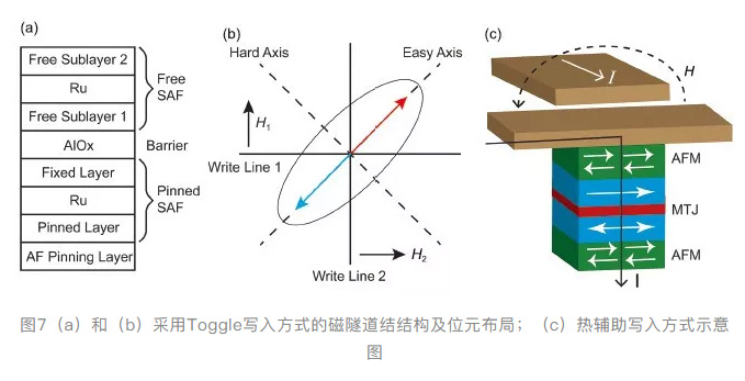
In order to overcome the star line constraint, Freescale proposed an improved magnetic field writing method called toggle. The magnetic tunnel junction based on this writing method uses a free layer of synthetic antiferromagnetic structure, as shown in Fig. 7(a). As shown, the hard (easy) magnetization axis of the free layer is placed at 45° to the write magnetic field. As shown in Fig. 7(b), a single write magnetic field cannot complete the magnetization reversal of the free layer, thereby avoiding " The semi-selected interference problem also extends the operational range of the write magnetic field.
Based on this toggle write method, Freescale successfully launched the first 4Mb toggle-MRAM commercial product. In addition to the toggle write mode, the academic community has also proposed the use of thermal assistance to improve the write performance of MRAM (Figure 7 (c)).
This type of writing requires only an applied magnetic field to solve the "semi-selected interference" problem, and the power consumption and reliability are improved. Although the heat-assisted MRAM overcomes the limitation of the star line to a certain extent, it also brings the complexity of the device integration process. In addition, since the heat treatment requires a special supporting process, considering the thermal conductivity, etc. The limitation of factors and the choice of materials are also limited to a certain extent.
Both thermal-assisted MRAM and toggle-MRAM can't fundamentally overcome the three inherent defects of magnetic field writing: 1) need milliamp level of write current, high power consumption; 2) with process size reduction The write current will increase sharply, and it is difficult to promote the application in the nano-scale magnetic tunnel junction; 3) the need for a long current-carrying metal wire to generate a magnetic field, and the circuit design complexity is high. These shortcomings limit the application prospects of MRAM. Therefore, the completion of magnetization reversal in purely electrical mode has become an important goal pursued by MRAM researchers at that time.
2. STT-MRAMIn 1996, Slonczewski and Berger theoretically predicted a purely electrical magnetic tunnel junction write method called spin transfer torque. The basic principle is shown in Figure 8. When current flows from the reference layer to the free layer, Firstly, the same spin angular momentum as the reference layer magnetization direction is obtained. When the spin-polarized current enters the free layer, the magnetization interaction with the free layer causes the lateral component of the spin-polarized current to be transferred, due to the conservation of the angular momentum. The transferred lateral component will act on the free layer in the form of a moment, forcing its magnetization direction to be close to the reference layer, which is called the spin transfer torque.
Similarly, for the current in the opposite direction, the reflection of the spin by the reference layer causes the free layer to magnetize to obtain the opposite moment. Therefore, the magnetization state to be written is determined by the direction of the current.

The spin transfer torque relies on the current to achieve magnetization reversal, the write current density is between 106~107A/cm2, and the write current can be reduced with the reduction of the process size, which overcomes the shortcomings of the traditional magnetic field write mode. Therefore, it is widely considered to be the best candidate for realizing the purely electrical writing method of the magnetic tunnel junction.
With the discovery of the spin transfer effect and the optimization of materials and structures, STT-MRAM devices based on the spin transfer effect have emerged. Since the spin transfer effect has been confirmed, on the one hand, researchers have tried a lot of efforts to reduce the critical current of magnetization reversal and increase thermal stability; on the other hand, Sony, Hitachi, Renesas, Crocus, Toshiba, Samsung, Hynix, IBM Many companies are also actively developing STT-MRAM.
In 2005, Sony first prepared a 4Kb STT-MRAM demo chip based on the CoFeB/MgO/CoFeB magnetic tunnel junction. Subsequently, Toshiba, Everspin, NEC, Hynix, Hitachi, and Tohoku University of Japan also prepared STT-MRAM samples.
Early magnetic tunnel junctions used In-Plane Magnetic Anisotropy. It has the following two drawbacks:
1) As the process decreases, thermal stability deteriorates. The storage lifetime of an in-plane magnetic anisotropic magnetic tunnel junction depends on the thermal stability barrier and the magnetic anisotropy field. The source of in-plane magnetic anisotropy is the aspect ratio of the film plane.
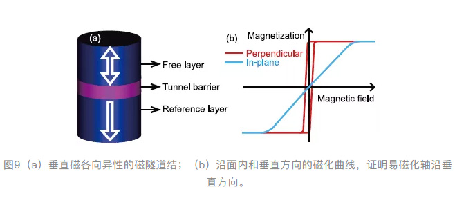
With the shrinkage of the process size (<50nm), the="" marginal="" effect="" of="" this="" film="" is="" intensified="">An effective way to solve the above two drawbacks is to use a magnetic magnetic tunnel junction of perpendicular magnetic anisotropy, as shown in FIG. The perpendicular magnetic anisotropy avoids the formation of the magnetic vortex at the edge of the film, and a high anisotropy field and thermal stability barrier can be obtained at the nanometer scale, thereby increasing the storage density. Moreover, if perpendicular magnetic anisotropy is employed, the critical inversion current required for the spin transfer torque is directly proportional to the thermal stability barrier.
Therefore, for the same thermal stability barrier, the perpendicular magnetic anisotropy can make the critical inversion current of the magnetic tunnel junction lower than the in-plane magnetic anisotropy, and accordingly, the inversion efficiency of the spin transfer torque is higher. In view of the above advantages, researchers have been working on the use of perpendicular magnetic anisotropy magnetic tunnel junction structure to build high-density, low-power pSTT-MRAM.
In 2002, Nishimura et al. first prepared a magnetic tunnel junction with perpendicular magnetic anisotropy. Its structure is TbFeCo/CoFe/Al2O3/CoFe/GdFeCo, and the writing mode is magnetic field driving. In 2006, Mangin et al. realized the perpendicular magnetic anisotropy and spin-transfer torque-driven magnetization reversal for the first time in a Co/Ni metal multilayer film.
In 2008, Toshiba prepared a magnetic tunnel junction with perpendicular magnetic anisotropy by using TbCoFe/CoFeB/MgO/CoFeB/TbCoFe structure, and realized spin transfer torque writing, but MgO was not fully presented due to insufficient annealing. In the single crystal state, the magnetic tunnel junction has a TMR value of only 15%.
In 2010, BM developed a 4Kb capacity STT-MRAM test chip based on a MgO barrier vertical anisotropic magnetic tunnel junction. In the same year, Hitach prepared a perpendicular magnetic anisotropic magnetic tunnel junction based on spin transfer torque, and its structure is Ta/CoFeB/MgO/CoFeB/Ta. The magnetic tunnel junction has high thermal stability and large The TMR value, as well as the lower critical inversion current, almost achieved the best performance at the time. Tr
Thereafter, the size of the perpendicular magnetic anisotropic magnetic tunnel junction continues to shrink to reduce the critical current density. The semiconductor CMOS circuit thus matched can also be made smaller in transistor size, thereby saving space and increasing the storage density. In 2011, Samsung reported a perpendicular magnetic anisotropic magnetic tunnel junction with a short axis length of only 17 nm.
The successful preparation of this size magnetic tunnel junction demonstrates the MRAM based on a perpendicular anisotropy magnetic tunnel junction that can be fused at the 22 nm node of the semiconductor process. In 2016, IBM and Samsung collaborated to show a perpendicular magnetic anisotropic magnetic tunnel junction with a diameter of 11 nm, which can be matched with the 14 nm node of the semiconductor process.
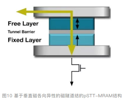
In the same year, IMEC demonstrated the world's smallest perpendicular magnetic anisotropic magnetic tunnel junction with a diameter of only 8 nm, which is compatible with semiconductor processes below 10 nm. Due to the simple structure and high integration of the “1 transistor + 1pMTJ” design (Fig. 10), the pSTT-MRAM is more competitive in the market.
At present, the latest low-power, high-capacity MRAM devices use perpendicular magnetic anisotropic magnetic tunnel junctions, such as Everspin's 256Mb STT-MRAM commercial products and the demonstrated 1Gb demonstration devices using perpendicular magnetic anisotropic magnetic Tunnel junction.
In addition to Everspin, companies such as IBM, Spin Transfer Technologies, Qaulcomm, and Samsung are also developing pSTT-MRAM device products. (Author: Zhu Lei)